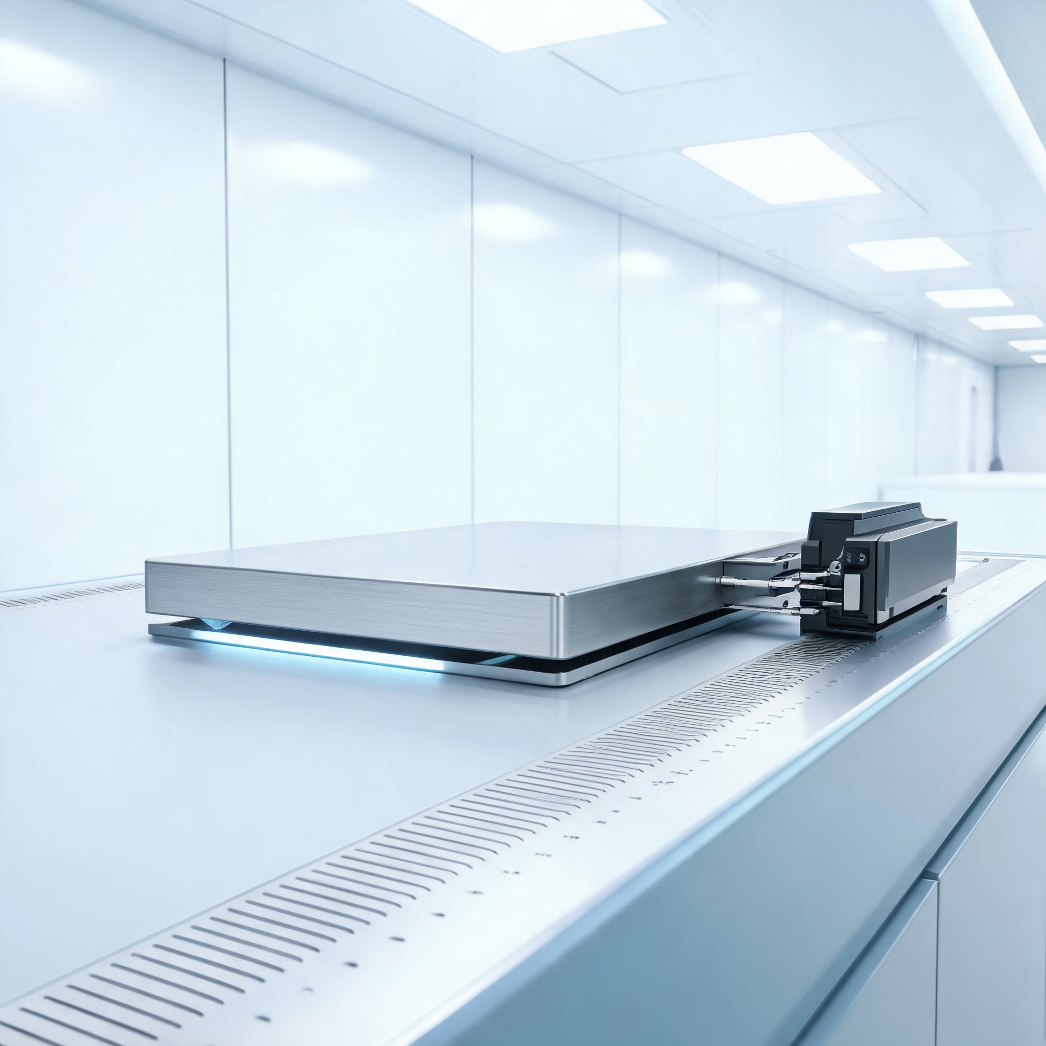
ETEL, part of HEIDENHAIN and a supplier of motion-control components and complete motion platforms, has introduced the METIS HP, a full air-bearing planar platform aimed at demanding step-and-scan semiconductor applications. The company lists direct laser writing and high-resolution optical inspection systems among the target uses.
According to ETEL, the platform is intended to combine speed and stability with dynamic straightness and projected tool-point measurement capability. At its core is a multi-degree-of-freedom (mDoF) HEIDENHAIN encoder. ETEL says this architecture maintains accuracy without thermal drift and enables projected tool-point measurement. The encoder is central to the platform’s positioning concept, and the company also links the architecture to trigger generation.
Trigger architecture
The company says its controllers can emulate a transistor-transistor logic (TTL) position signal for use as a trigger event. ETEL positions this approach as an alternative to the classical interferometer used as an advanced trigger generator. According to the company, the METIS HP removes the need for a mirror on the carriage and avoids air lensing and air perturbation effects, while also lowering cost.
Scanning performance
ETEL cites ±150 nm accuracy over the full XY stroke after mapping and ±150 nm dynamic straightness at speeds up to 1 m/s. The platform’s dynamic capabilities reach accelerations up to 20 m/s². ETEL says these characteristics reduce turnaround time and increase machine throughput in step-and-scan applications.
For high-end inspection in advanced packaging, the company says rapid and precise focal-distance adjustment is required. METIS HP includes a high-bandwidth 4-DoF module for fine control of the Z, tip, tilt and theta axes. ETEL describes the platform as suited to these inspection tasks.
Large-area processing
Stéphane Pellegrini, product manager at ETEL, said the METIS HP builds on the company’s experience in high-precision platforms and provides the trajectory quality needed for advanced optical processes. He said its speed stability and dynamic straightness are intended to maintain consistent performance at high scanning velocities. According to Pellegrini, the platform supports panel sizes up to 600 mm × 600 mm and addresses demand for next-generation maskless lithography on large-area substrates.
ETEL’s announcement presents METIS HP as a motion platform for semiconductor scanning. The stated design targets are precision, dynamic stability and trigger integration, with the 4-DoF module adding fine adjustment for focal distance. The company’s performance figures are presented as platform specifications after mapping.
The platform is aimed at applications where scanning motion supports optical processes, including direct writing and inspection. The announcement focuses on the motion subsystem and the specifications ETEL provides for those uses.